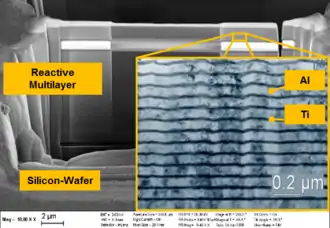
Reactive bonding describes a wafer bonding procedure using highly reactive nanoscale multilayer systems as an intermediate layer between the bonding substrates. The multilayer system consists of two alternating different thin metallic films. The self-propagating exothermic reaction within the multilayer system contributes the local heat to bond the solder films. Based on the limited temperature the substrate material is exposed, temperature-sensitive components and materials with different CTEs, i.e. metals, polymers and ceramics, can be used without thermal damage.
Overview

The bonding is based on reactive nano scale multilayers providing an internal heat source. These foils are combined with additional solder layers to achieve bonding. The heat that is required for the bonding is created by a self-propagating exothermic reaction of the multilayer system. This reaction is ignited by an energy pulse, i.e. temperature, mechanical pressure, electrical spark or laser pulse. The generated heat is localized to the bonding interface and limited due to a short term heating phase within milliseconds.
This heat is an advantage of this approach, so the used materials are not exposed to high temperatures and allow rapid cooling.[1] A drawback is that this approach is not applicable for bond frame dimensions of few ten micrometres. This is based on the limited handling and structuring abilities of the foils at this small dimensions.[2]
The material used for multilayer systems is a bilayer of alternating elements, commonly Ni/Al, Al/Ti or Ti/a-Si.[1] The metallic layer is usually 1 to 30 nm thick and can be arranged as horizontal or vertical nano scale material films and are a combination of a reactive and a low melting component.[2] With increased bilayer thickness, the reaction velocity decreases and the reaction heat increases. Therefore, a specific balance between high reaction velocity and high reaction heat is necessary.[3]
A commercial example of such material is NanoFoil. The corresponding bonding process is known as NanoBond.
Procedural steps
Preprocessing
Two different reactive structures are established, conventional lateral layer-by-layer (multilayer) and vertical arranged structures.[2] Based on difficulties, that occur during handling, patterning and positioning of the freestanding foils, the multilayer films are directly deposited onto the silicon substrate.[4] The deposition of the multilayer systems on silicon is achieved by magnetron sputtering, electroplating or etching. The vertical nano structures are also created directly on the substrate surface.[2]
The substrate surfaces are deposited with a solder layer, i.e. gold (Au), using physical vapor deposition (PVD). The PVD process promotes the wetting of the solder.[1] The intermixing of the used components during deposition influences the reaction parameters and to prevent this the substrates are cooled.[4]
A commonly used deposition method for multilayer structures is magnetron sputtering. A multilayer system consists of thousands of thin single layers of the component combination that are alternately sputtered on the substrate surface.
For electroplating or electrochemical deposition (ECD) multilayer deposition two approaches are established. On the one hand a two bath method exist, which means an alternating deposition in two different plating baths. On the other hand, a one bath method, with an electrolyte containing both film components in one bath, can be used. The ECD process reduces process time and complexity. In addition, this method enables pattern plating to prevent complex etching process of structures.
Vertical nanostructures are created in two steps. At first, needles in the silicon substrate are created by dry etching. The other used material is deposited using sputtering to cover those needles. This approach reduces the process time and complexity drastically due to the deposition omission of the thousands of single layers.[2] Further, reactive foil patterning can be realized by applying an electrochemical machining process.
Bonding


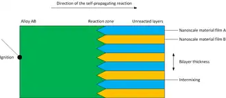
The bonding process is based on the reaction of the nanoscale multilayer to release energy concentrated at the interface.[1] The self-propagating reaction is caused by the reduction of chemical bond energy in the multilayer system (compare to figure "Schematic self-propagating reaction in a multilayer system after ignition").
The system alloy, or an intermetallic compound, (AB) is formed from the intermixing elements (A+B) due to atomic diffusion.[2]
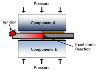
The reactive foil is ignited by an energy pulse resulting in an immediate self-propagating reaction (compare to figure "Schematic reactive bonding process with a reactive multilayer as heat source").
This local intermixing process produces heat that is transmitted to the adjacent element layers. The reaction spreads through the foil in milliseconds.[4] This energy release leads to a high temperature in the bonding interface. Meanwhile, the components outside the interface are not exposed to the high temperatures of the reaction.[1] Besides the high interface energy, this reaction is also promoted by the low thickness and therefore the reduced diffusion path of the single metallic layers.[2]
The resulting internal heat melts the solder layers to form a bond with the multilayer system and the substrate based on diffusion.[5] This exothermic reaction can be ignited in reactive materials like compacted powders, e.g. Ni/Ti or Ti/Co, as well as in nanostructured multilayer systems, e.g. Ni/Al.[4] The bonding can take place in various environments, i.e. vacuum,[6] with a force providing a defined mechanical pressure[1] at room temperature.[4] A high applied mechanical pressure enhances the solder flow and therefore can improve the wetting of the substrate.[5]
Examples
Reactive bonding approach is used to assemble MEMS components including die attachment and the hermetic sealing of micro-system packages.[1] The process is used to join temperature sensitive biological activated substrates for diagnostics or medical devices. In addition disposable microfluidic devices with sensing function and immobilized cells can be fabricated.[2]
Technical specifications
| Materials |
Substrate:
Solder:
Reactive component:
|
| Temperature |
|
| Advantages |
|
| Drawbacks |
|
See also
References
- 1 2 3 4 5 6 7 Böttge, B. and Bräuer, J. and Wiemer, M. and Petzold, M. and Bagdahn, J. and Gessner, T. (2010). "Fabrication and characterization of reactive nanoscale multilayer systems for low-temperature bonding in microsystem technology". Journal of Micromechanics and Microengineering. Vol. 20, no. 6.
{{cite news}}: CS1 maint: multiple names: authors list (link) - 1 2 3 4 5 6 7 8 9 Lin, Y.-C. and Baum, M. and Haubold, M. and Frömel, J. and Wiemer, M. and Gessner, T. and Esashi, M. (2009). "Development and evaluation of AuSi eutectic wafer bonding". Solid-State Sensors, Actuators and Microsystems Conference, 2009. TRANSDUCERS 2009. International. pp. 244–247. doi:10.1109/SENSOR.2009.5285519.
{{cite conference}}: CS1 maint: multiple names: authors list (link) - ↑ Qiu, X. & Wang, J. (2008). "Bonding silicon wafers with reactive multilayer foils". Sensors and Actuators A: Physical. 141 (2): 476–481. doi:10.1016/j.sna.2007.10.039.
- 1 2 3 4 5 6 Wiemer, M. and Bräuer, J. and Wünsch, D. and Gessner, T. (2010). "Reactive Bonding and Low Temperature Bonding of Heterogeneous Materials". ECS Transactions. 33 (4): 307–318. Bibcode:2010ECSTr..33d.307W. doi:10.1149/1.3483520. S2CID 96914667.
{{cite journal}}: CS1 maint: multiple names: authors list (link) - 1 2 Wang, J. and Besnoin, E. and Knio, O. M. and Weihs, T. P. (2004). "Investigating the effect of applied pressure on reactive multilayer foil joining". Acta Materialia. 52 (18): 5265–5274. Bibcode:2004AcMat..52.5265W. doi:10.1016/j.actamat.2004.07.012.
{{cite journal}}: CS1 maint: multiple names: authors list (link) - ↑ Qiu, X. and Welch, D. and Christen, J. and Zhu, J. and Oiler, J. and Yu, C. and Wang, Z. and Yu, H. (2010). "Reactive nanolayers for physiologically compatible microsystem packaging". Journal of Materials Science: Materials in Electronics. 21 (6): 562–566. doi:10.1007/s10854-009-9957-5. S2CID 137116832.
{{cite journal}}: CS1 maint: multiple names: authors list (link)